
ZhongLian
- Author:
- Source:
- Date: 2023-04-24
- Views: 108Times
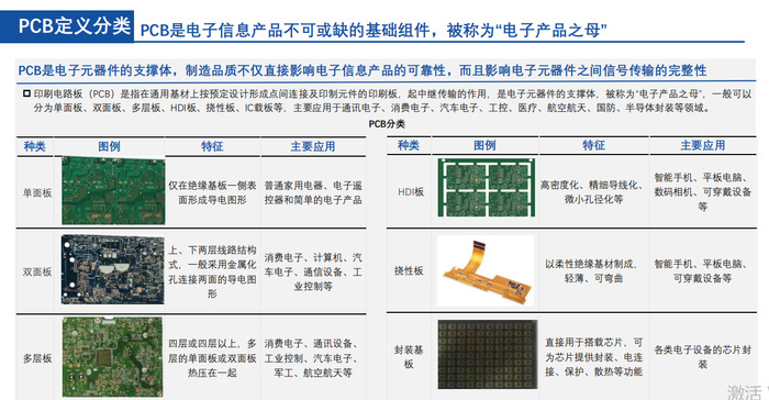 PCB: Printed Circuit Board (PCB) refers to a printed board that forms point-to-point connections and printed components on a general-purpose substrate according to a predetermined design. Its main functions are: 1) Provide various components in the circuit mechanical
Support; 2) Make various electronic components form the electrical connection of the predetermined circuit, and play the role of relay transmission; 3) Mark the installed components with marking symbols, which is convenient for insertion, inspection and debugging.
u Copper Clad Laminate (CCL for short): The full name is copper clad laminate. Copper clad laminate is the core material for making printed circuit boards, and it is responsible for the three functions of conductive, insulating and supporting printed circuit boards. copper clad laminate
Quality determines the performance, quality, processability in manufacturing, manufacturing level, manufacturing cost and long-term reliability of printed circuit boards.
u FR-4: flame retardant epoxy resin glass fiber cloth base copper clad laminate.
u HDI: The abbreviation of "High Density Interconnect", that is, "High Density Interconnection", a high-density printed circuit board technology using thin lines, tiny holes, and thin dielectric layers.
u Rigid board: A printed circuit board made of a rigid base material that is not easy to bend and has a certain degree of toughness.
u Flexible board (FPC): also known as flexible board, is a printed circuit board made of flexible insulating substrates such as polyimide or polyester film. The flexible board can be bent, wound, folded, and can be layout requirements to be arranged and in 3D
The space moves and expands, so as to achieve the integration of component assembly and wire connection.
u Multi-layer board: multi-layer board is a printed circuit board with four or more layers. The multi-layer single-sided or double-sided boards are hot-pressed together, and formed between different layers through secondary drilling and hole metallization. a conductive path.
u IC package substrate (IC Package Substrate): also known as IC package substrate, the package substrate is the key carrier in the packaging and testing link of the integrated circuit industry chain, which can realize multi-pin, reduce the area of packaged products, improve electrical performance, and achieve high
densification etc.
u SLP (substrate-like PCB): referred to as Substrate-like PCB (SLP) in Chinese, it is the main force of the next generation PCB board. 40/50 microns shortened to 20/35
Micron, from the perspective of manufacturing process, SLP is closer to the IC substrate used for semiconductor packaging, but it has not yet reached the specifications of the IC substrate, and its purpose is still to carry various active and passive components, so it still belongs to the category of PCB. Electronic element
The number of devices carried can reach twice that of HDI.
Previous: Introduction to PCB testing
Next: PCB Etchback Techniques


Copyright © Yiwu Zhonglian Technology Co., LTD
TEL: 0755-26395762 / 26395736 Whatsapp: 86-166 7150 6201
Add: Sufu Road, Suxi Town, Yiwu Industrial Park, Zhejiang Province .China. Postcode: 322023
- 在线服务
-

网站建设维护