
ZhongLian
- Author:
- Source:
- Date: 2023-04-24
- Views: 91Times
 Why do you have made a PCB panel ?
1. In order to meet the needs of production. Some PCB boards are too small to meet the requirements for making fixtures, so they need to be put together for production.
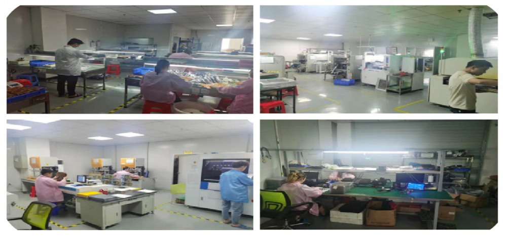
2. Improve the welding efficiency of SMT patch. Only one SMT is required to complete the welding of multiple PCBs.
3. Improve cost utilization. Some PCB boards are special-shaped, and jigsaw boards can use the PCB board area more efficiently, reduce waste, and improve cost utilization.
2 What are the ways of jigsaw puzzle design?
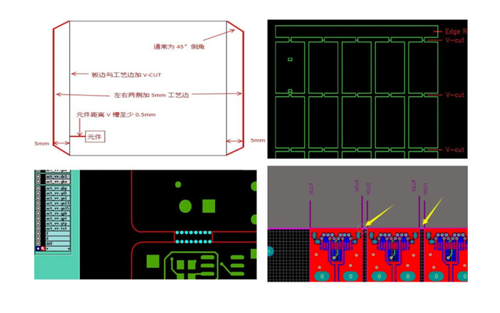
1. V-CUT
V-CUT is to draw a groove at the joint of the two boards, as long as the two boards are put together, there is a gap between them (usually 0.4mm), but the connection of the boards in this place is relatively thin and easy to break , When jigsawing, the edges of the two boards need to be merged together.
V-CUT is generally a straight line, there will be no complicated routing such as curved arcs, and try to be on a straight line when making boards.
2. Stamp hole
For irregular PCB boards, such as circular ones, V-CUT cannot do it. At this time, stamp holes need to be used for panel connection, so stamp holes are generally used in special-shaped boards.
The edges of the two boards are connected by a small board, and there are many small holes in the connection between this small board and the two boards, which is easy to break. After breaking off, the edge of the board is like the edge of a stamp, so this way of jigsaw puzzle is called stamp hole.
3. Hollow connecting strip
Hollow connecting strips are mostly used in boards with half-hole technology. They are connected by very narrow plates, which are somewhat similar to stamp holes. The difference is that the connecting part of the connecting strip is narrower and there are no holes on both sides.
There is a disadvantage of the jigsaw method of the hollow connecting strip: there will be an obvious bump after the board is broken. The stamp holes also have bumps, which are not so obvious because they are separated by vias.
Some people may think that it is not enough to use stamp holes directly, why use hollow connecting strips? This is because when making a module with half-holes all around, neither the stamp hole nor the V-CUT can be used, and can only be connected at the four corners of the module through hollow connecting strips.
3 What is the principle of jigsaw puzzle?
In order to facilitate production, try to keep the boards in a square shape after paneling. In short, don't let the aspect ratio gap be too large
4 spacing requirements
1. For the PCB whose outermost distance from the edge of the board is less than 3mm, the process side must be processed, usually the longer side is used as the process side;
2. A space >0.5mm should be reserved between components and V-CUT to ensure the normal operation of the tool.


Copyright © Yiwu Zhonglian Technology Co., LTD
TEL: 0755-26395762 / 26395736 Whatsapp: 86-166 7150 6201
Add: Sufu Road, Suxi Town, Yiwu Industrial Park, Zhejiang Province .China. Postcode: 322023
- 在线服务
-

网站建设维护